Image
Showing 11 - 20 of 47 results
University of Manitoba
Live rodent and material imaging using optical, micro-CT, PET, MRI, PET-MRI and ultrasound imaging
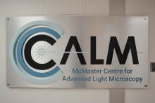
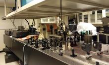
McMaster University
Fosters academic and industrial partnerships through access to cutting-edge light microscopy, photopatterning, and light-assisted 3D printing techniques.
University of Victoria
Materials science.
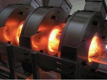
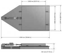
University of Victoria
Materials science and engineering. The facility allows the growth (production) of bulk single crystal materials that have used in various electronic and optoelectronic device developments.
Image
University of Manitoba
Characterization of minerals in relation to geochemical and environmental processes
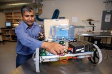
Carleton University
Soil and foundation improvement solutions for seismic-resistant design, geo-hazards investigation and mitigation
Image
University of Alberta
Rock physics and mechanics, surface and borehole geophysics
University of Victoria
Supports the development of innovative and sustainable construction materials well suited to new construction and repair/rehabilitation projects
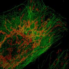
University of Alberta
Offers access to, and training for, state-of-the-art quantitative light and electron microscopy
University of Alberta
Offers state-of-the-art analytical flow cytometry, cell sorting, and data analysis.