Materials characterization and consultation to determine structural and compositional information on the micron to nano/atomic-scale using electron and ion microscopy.
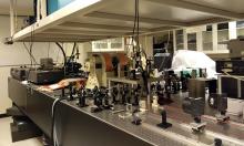
Fosters academic and industrial partnerships through access to cutting-edge light microscopy, photopatterning, and light-assisted 3D printing techniques.
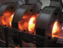
Materials science and engineering. The facility allows the growth (production) of bulk single crystal materials that have used in various electronic and optoelectronic device developments.
Develops new approaches and tools for protecting information systems and their data against malicious hacking activities (information and system security)