Materials characterization and consultation to determine structural and compositional information on the micron to nano/atomic-scale using electron and ion microscopy.
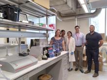
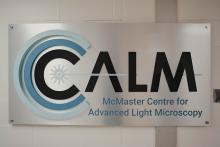
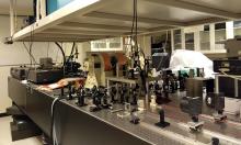
Fosters academic and industrial partnerships through access to cutting-edge light microscopy, photopatterning, and light-assisted 3D printing techniques.
Celebrates and develops imaginative practices/programs in schools/workplaces/communities; collaborates with organizations to increase imaginative engagement/innovation
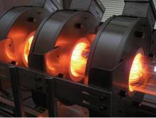
Materials science and engineering. The facility allows the growth (production) of bulk single crystal materials that have used in various electronic and optoelectronic device developments.